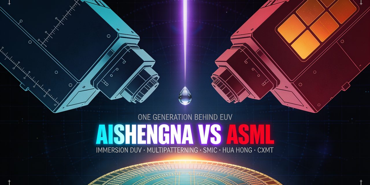
Shanghai Aishengna Electronic Technology Group has emerged as the company behind China’s latest attempt to produce domestic immersion DUV lithography machines. Lithography remains one of the largest weaknesses in China’s semiconductor supply chain. It does not mean that Aishengna has suddenly become the new ASML. The Chinese company still has to prove that its systems can deliver the precision, productivity, reliability and manufacturing yield required inside a commercial chip factory.
There is a distinction between producing a machine and matching ASML. A working scanner can demonstrate technical progress. A competitive scanner must expose hundreds of wafers per hour, align many chip layers with extraordinary accuracy and operate reliably for long periods of time. It must also be supported by software, metrology, spare parts and engineers who can keep production running.
What is known about Shanghai Aishengna
Reuters identified Shanghai Aishengna Electronic Technology Group on July 28, 2026 as the state owned company leading China’s immersion DUV production effort. According to an anonymous source familiar with the programme, Aishengna incorporated teams from Chinese lithography developers including Yuliangsheng and Shanghai Micro Electronics Equipment. The company was established in August 2023 with registered capital of 7 billion yuan. Its shareholders are connected to Shanghai Electric Holding and Shanghai International Trust.
Public information about Aishengna remains extremely limited. The company does not appear to have a public website that explains its technology, product specifications or development roadmap. The reported progress has also not been confirmed on the record by Aishengna or its intended customers.
The reported delivery targets are approximately five immersion DUV systems in 2026 and around twenty in 2027. The first machines are expected to go to SMIC, Hua Hong Semiconductor and memory producer ChangXin Memory Technologies. Reuters noted that the scanners still require further testing and remain far from matching competing ASML products.
Why immersion DUV lithography matters
Immersion deep ultraviolet lithography uses 193 nanometre light and places a thin layer of water between the projection lens and the wafer. The water increases the effective numerical aperture and allows smaller features to be printed than with dry DUV systems.
An immersion DUV machine can print features suitable for advanced semiconductor manufacturing. Chipmakers can also use multiple exposures and additional processing steps to produce smaller structures. This technique is known as multi patterning. It helped SMIC manufacture 7 nanometre class processors without access to EUV equipment. However, every extra patterning step adds complexity, production time and extra risk for defects. This usually means higher costs and lower yields than a process designed around EUV lithography.
Domestic DUV production would give China something strategically valuable even if the machines are less efficient than ASML systems. Chinese foundries would gain an alternative source of equipment if Western governments impose stricter controls on exports, software updates, spare parts or maintenance services. The immediate objective may not be to win international customers. It may simply be to keep Chinese production lines operating under increasingly restrictive conditions.
The performance gap with ASML
ASML is not standing still while Shanghai Aishengna develops its first production systems. The Dutch company continues to improve DUV productivity, imaging quality and overlay accuracy. Its latest NXT 2150i immersion scanner offers better imaging, a 15 percent improvement in overlay performance and a 5 percent increase in throughput compared with its predecessor. ASML reported in April 2026 that the system was operating at more than 300 wafers per hour with overlay performance below one nanometre.
These numbers illustrate the real competitive barrier. Overlay measures how accurately one chip layer is positioned on top of another. A scanner can produce very small features and still be unsuitable for advanced manufacturing if those features are not aligned consistently across many layers and thousands of wafers.
Throughput is equally important. A machine that produces acceptable test wafers but processes them too slowly can increase the cost of every chip. Reliability also affects factory economics. An advanced wafer fabrication plant is designed to operate continuously. Unexpected downtime can disrupt the entire production flow. Aishengna must prove its scanners under these conditions before its products can be considered equivalent to ASML’s immersion systems.
ASML sells more than scanners
ASML’s position is also supported by a broad product and service ecosystem. The company combines lithography systems with computational lithography, process control, metrology, inspection, upgrades and field service. In 2025, ASML generated €32.7 billion in total sales. Service and field option sales reached €8.2 billion, reflecting the importance of its installed machine base and customer support operations. The company also spent €4.7 billion on research and development during that year.
Shanghai Aishengna is not merely trying to reproduce one machine. It is competing with decades of production data, supplier relationships, intellectual property and experience gained by supporting fabs around the world. Building a national service network inside China may be possible. Reaching ASML’s accumulated process knowledge will take much longer.
DUV success would not create an EUV rival
The comparison with ASML becomes even less convincing when EUV lithography is included. ASML remains the only company supplying EUV scanners for commercial chip production. These machines use 13.5 nanometre light and are required to print the most complex layers of leading processors and memory chips with fewer patterning steps. ASML is already deploying High NA EUV systems designed for future 2 nanometre logic processes and advanced memory production.
China is reportedly working on domestic EUV technology, but the obstacles are different from those involved in DUV. Analysis from The Diplomat identifies three particularly important barriers. China needs a sufficiently powerful and stable EUV light source, mirrors with extreme surface precision and photoresist chemicals with exceptional purity. Current Chinese research may be narrowing individual gaps, but combining all components in a reliable production scanner is a much harder challenge.
The optical system alone shows the level of complexity. EUV light is absorbed by air and conventional lenses. The scanner must therefore operate in a vacuum and use multilayer mirrors. Even tiny surface irregularities can create imaging errors. ZEISS describes its EUV mirrors as some of the most precise optical components ever manufactured.
ASML’s experience also shows how long the transition from prototype to commercial production can take. The company shipped its first EUV demonstration system in 2006. Its first production model followed in 2013 and broader customer adoption only accelerated several years later. Producing a prototype is therefore the beginning of industrial development rather than its final stage.
How to measure Aishengna’s progress
Announcements and production targets reveal ambition, but they do not provide enough information to judge product quality. The most useful indicators will come from customer factories. Important questions include:
- Can the scanners maintain overlay accuracy during continuous production?
- How many wafers can each machine process per hour?
- What defect rates and chip yields do customers achieve?
- How often do the machines require maintenance or calibration?
- Are critical optics, lasers, stages and control systems produced domestically?
- Can Aishengna manufacture dozens of consistent systems rather than a few individual units?
CSIS has argued that lithography announcements should be judged by throughput and commercial usefulness rather than precision claims alone.
How to read Chinese lithography announcements
When Hangzhou announced the Xizhi electron beam lithography machine with claimed 0.6nm precision and 8nm line width, Chinese media framed it as sidestepping ASML’s dominance. Electron beam systems are maskless and flexible, but they draw patterns point by point, which makes them far too slow for volume production.
Analysts at CSIS have described why such claims multiply. State capital arrives in large waves with limited regard for efficiency, which produces duplication and projects that stall after the funding is booked. Local governments and firms have every incentive to advertise progress, because good news buys recognition and budget in Beijing. Externally, the timing of announcements often tracks moments of geopolitical pressure. Meanwhile the measurable reality has been modest. SMEE, China’s leading domestic supplier, sells i-line and some DUV tools and holds around four percent of the global i-line market. Huawei linked SiCarrier is reportedly working toward 28nm capability.
Aishengna fits a recognisable move in that landscape, the state stitching scattered ventures into one national champion. That consolidation is important. It concentrates talent and funding instead of scattering it. It is also the point at which the programme becomes measurable, since a national champion has to ship.
A strategic challenger rather than a second ASML
Shanghai Aishengna Electronic Technology Group is not yet the new ASML. It has not demonstrated equivalent DUV performance and it does not offer commercial EUV technology. Its reported production scale is also tiny compared with ASML’s global operations.
That does not make the company irrelevant. If Aishengna can supply usable immersion DUV systems to major Chinese foundries, it will reduce a critical dependency and establish a foundation for further improvement. Its first important role may be that of a protected domestic supplier rather than a global market leader. The real test will not be whether five machines leave a factory in 2026. It will be whether Chinese chipmakers are still using them efficiently and economically several years later.